






Key Points
- Bluehill VC leads Rs 10.2 crore seed round in Makr Microsystems with Artha Venture Fund
- Makr develops acoustic atomic force microscopy for subsurface semiconductor inspection
- Investment follows Bluehill maiden fund close at Rs 400 crore
Bluehill VC, a Chennai-based venture capital firm focused on frontier technology, has led a Rs 10.2 crore seed funding round in Makr Microsystems, a Bengaluru-based semiconductor metrology startup developing technology to detect defects beneath chip surfaces.
Artha Venture Fund participated in the round, which will support Makr’s technology development, customer validation and commercial deployment efforts. The investment marks Bluehill’s third bet in the semiconductor sector and comes weeks after the fund announced the final close of its maiden fund at Rs 400 crore.




Makr is developing a measurement system that allows chipmakers to visualise and measure structures buried beneath the surface of semiconductor devices. As chip architectures become more complex, with multiple layers stacked vertically, the ability to inspect what lies beneath the surface without destroying the chip has become increasingly valuable for quality control and yield improvement.
Makr subsurface imaging
The company’s core technology is Acoustic Atomic Force Microscopy, or AAFM. This combines atomic force microscopy, a technique that scans surfaces at the nanometre scale using a physical probe, with acoustic sensing that can penetrate below the surface layer. The acoustic signals provide information about structures, interfaces and defects that conventional surface-based inspection tools cannot access.
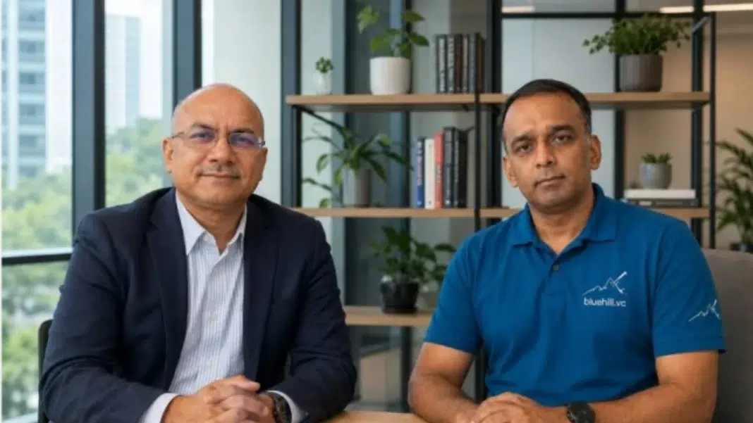
Manu Iyer, general partner, Bluehill VC, said the fund was looking for companies positioned deeper in the semiconductor value chain. “We are excited about companies that sit deeper in critical technology value chains. Makr is solving a difficult problem in semiconductor manufacturing at a time when the industry is moving toward increasingly complex architectures,” he said.
“We believe this is a global opportunity, and that world-class semiconductor equipment and technology can be built from India,” Iyer added.
The technology targets several applications in advanced semiconductor manufacturing. These include advanced packaging, where multiple chips are combined into a single package; hybrid bonding, a technique for joining chips with extremely fine connections; and inspection of chiplet interconnects, the interfaces between small chip modules designed to work together.
Ashwin Lal, founder, Makr Microsystems, said the need for subsurface measurement was growing as chip designs evolved. “Semiconductor manufacturing is creating structures that are increasingly difficult to see and measure. As architectures move into the third dimension, understanding what is happening beneath the surface becomes critical to improving yield,” Lal said.
“Our goal is to make the subsurface measurable, non-destructively and at the resolution the next generation of chipmaking demands,” he added.
Founder background
Lal holds an MSc in Physics from IIT Kanpur and a PhD in Microtechnology from EPFL, the Swiss Federal Institute of Technology in Lausanne. He previously founded Shilps Sciences and worked as an engineer at Applied Materials, a major semiconductor equipment manufacturer. The broader team includes specialists in semiconductor metrology, atomic force microscopy, MEMS and embedded systems.
The investment shows growing investor interest in the less visible parts of the semiconductor supply chain. While much attention has focused on chip design companies and manufacturing plants, the equipment, materials and measurement technologies that enable chipmaking are equally critical to the industry’s functioning.
By the numbers
- Rs 10.2 crore
- Seed funding raised by Makr Microsystems
- Rs 400 crore
- Bluehill VC maiden fund size
India Semiconductor Mission 2.0, the government’s expanded programme for building domestic semiconductor capabilities, includes support for equipment, materials and research alongside its focus on fabrication plants and design centres. The mission aims to develop a broader ecosystem rather than focusing solely on the most capital-intensive manufacturing facilities.
Bluehill has positioned itself to invest across this ecosystem. The fund invests from seed to Series A stage across defence, space, semiconductors, advanced materials, energy, manufacturing, industrial internet of things and robotics. It was founded in 2024 by Iyer and Sridhar P.
For Makr, the opportunity extends beyond India. The same shift toward complex chip architectures is occurring across semiconductor manufacturing hubs worldwide, from Taiwan and South Korea to the United States and Europe. Demand for better inspection tools is growing wherever advanced chips are being made or packaged.
The seed round will allow Makr to continue developing its technology platform and begin validation with potential customers in the semiconductor industry. The company said it aims to demonstrate that its acoustic imaging approach can deliver the resolution and reliability required for production use.
Your Questions, Answered
What does Makr Microsystems do?
Makr Microsystems develops semiconductor metrology technology using Acoustic Atomic Force Microscopy to detect defects and measure structures beneath the surface of chips without damaging them.
How much funding did Makr Microsystems raise?
Makr Microsystems raised Rs 10.2 crore in seed funding led by Bluehill VC with participation from Artha Venture Fund.
What is Acoustic Atomic Force Microscopy?
Acoustic Atomic Force Microscopy combines atomic force microscopy, which scans surfaces using a physical probe, with acoustic sensing that can penetrate below the surface to reveal buried structures and defects.
Who founded Makr Microsystems?
Ashwin Lal founded Makr Microsystems. He holds a PhD in Microtechnology from EPFL and previously worked at Applied Materials and founded Shilps Sciences.


